Custom STM32 Dev Board
A STM32F107RCTx-based development board with USB and SWD interfaces, designed for embedded prototyping.
Project Overview
The goal was to create a low-cost, compact STM32-based dev board with all essential interfaces exposed—USB, SWD, and mapped I/Os—along with three user/debug LEDs.
Technologies Used
- KiCad PCB Design Suite
- STM32CubeIDE
Schematic Design
Microcontroller Selection
STM32F107RCTx was selected for its integrated USB peripheral and rich I/O set.
Power Supply Unit (PSU)
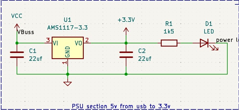
Linear PSU based on the ASM1117-3.3 voltage regulator was used to step down the +5V from the USB to 3.3V. C1 and C2 are the input and output smoothing capacitors. R1 is the 1.5kΩ current limiting resistor for the LED D1, which serves as the power indicator.
Microcontroller Decoupling Capacitors
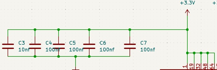
In this design C3, C4, C5, C6 and C7 are decoupling capacitors for the microcontroller. Their primary function is to stabilize the supply voltage by acting as local energy reservoirs. During operation the microcontroller can draw sudden bursts of current due to internal switching. This current can briefly dip the voltage on the power rail potentially leading the microcontroller to brown out or cause erratic behavior. C4, C5, C6 and C7 are 100nF ceramic capacitors chosen for their effectiveness in filtering high frequency noise, C3 is a complementary 10nF ceramic capacitor included to further filter the higher frequencies and transients.
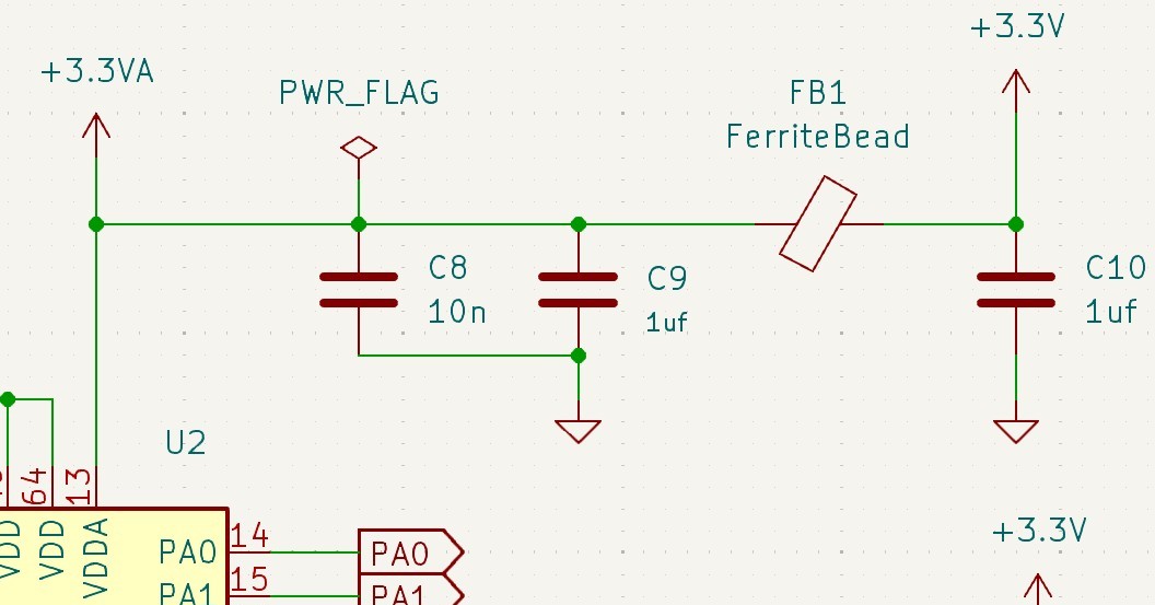
Analogue Voltage Stabilisation and Filtering
Ferrite beads and capacitors were used to stabilize the analog supply for precision components.
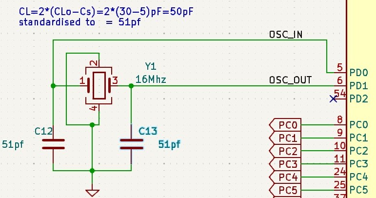
Crystal Oscillator Circuit
The crystal's load capacitance (CL) was taken from the datasheet, which specifies a value of 30 pF — this is the capacitance required for the crystal to oscillate at its rated frequency. Stray capacitance (Cs), which includes PCB trace, pin, and parasitic capacitances, was estimated at 5 pF, a typical value for a 2-layer FR-4 board with short crystal traces.
To find the required capacitor value C for C12 and C13, the formula C = 2 × (CL − Cs) was applied. Substituting the values gives: 2 × (30 pF − 5 pF) = 50 pF. The nearest standard capacitor value, 51 pF, was selected for C12 and C13.
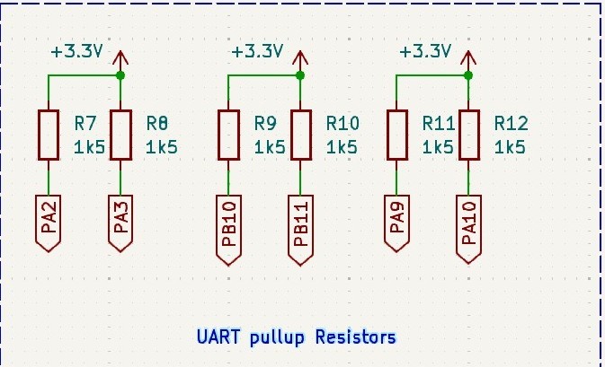
UART Pullup Resistors
The dedicated UART pins PA2, PA3, PB10, PB11, PA9, PA10 are tied to the 3.3V rail via the resistors (R7–R12). This prevents these pins from floating into an unknown state during device power-up/reset which may be interpreted as a transmission of garbage data. A 10K resistor value was chosen as it provides stable signal integrity while drawing a small amount of current (~0.33 mA) when the pin is driven low.
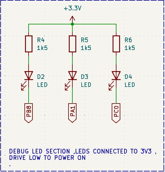
Debug and LED Circuit
The LEDs (D2, D3, and D4) are utilised for visual debugging and status checks. Each LED anode is tied to the 3.3V rail via its respective current-limiting resistor (R4, R5, and R6). The cathodes are driven via the microcontroller pins PB8, PA1 and PC0. The LEDs are illuminated by driving the microcontroller pins low (0V), sinking the current.

I/O Mapping
Common GPIOs were routed to headers for flexibility in testing peripherals. The LEDs D2, D3, and D4 along with their limiting resistors R4, R5, and R6 were mapped accordingly.
PCB Layout
Layer Count & Dimensions

A 2-layer PCB design was used to minimize cost. Final dimensions: 80mm x 50mm.
MCU Placement

The microcontroller was centrally placed to reduce trace lengths to supporting components.
PCB Fabrication
ThePCBs were Fabricated by JLCPCB — . 5 boards delivered days.
| Order Summary | |
|---|---|
| Order Number | Y7-4598312A |
| PCB Quantity | 5 |
| Build Time | 3 days |
| Product Type | Industrial / Consumer Electronics |
| Different Designs | 1 |
| Delivery Format | Single PCB |
| Board Specifications | |
| Base Material | FR-4 |
| Material Type | TG135 |
| Layers | 2 |
| Dimensions | 98 mm × 55 mm |
| PCB Thickness | 1.6 mm |
| Outer Copper Weight | 1 oz |
| Stackup | Not specified |
| Finish & Appearance | |
| PCB Color | Green |
| Silkscreen | White |
| Silkscreen Technology | Ink-jet / Screen Printing |
| Surface Finish | ENIG |
| Gold Thickness | 1U" |
| Appearance Quality | IPC Class 2 Standard |
| Mark on PCB | Remove Mark |
| Package Box | With JLCPCB logo |
| Via & Hole Details | |
| Via Covering | Untented |
| Min Via Hole Size / Diameter | 0.3 mm / (0.4 / 0.45 mm) |
| Via Plating Method | Not specified |
| Blind Slot | No |
| Castellated Holes | No |
| Countersink Hole | No |
| Gold Fingers | No |
| Edge Plating | No |
| Deburring / Edge Rounding | No |
| Board Outline Tolerance | ±0.2 mm (Regular) |
| Testing & Compliance | |
| Electrical Test | Flying Probe — Fully Tested |
| Confirm Production File | Yes |
| 4-Wire Kelvin Test | No |
| Inspection Report | No |
| UL Marking | No |
| Paper Between PCBs | No |
BOM & Component Sourcing
Components were sourced from DIGIKEY ,the plan was to assemble all 5 PCBs ,additional components were also added for redundancy,just incase a component was dammaged or lost
| Description | Qty | Unit Price | Extended Price |
|---|---|---|---|
| CAP CER 22UF 10V X5R 0805 | 12 | $0.17 | $2.06 |
| CAP CER 0805 10NF 100V C0G 10% | 20 | $0.23 | $4.56 |
| CAP CER 100NF 100V X8L 0603 | 30 | $0.16 | $4.65 |
| CAP CER 1UF 16V X7R 0603 | 12 | $0.04 | $0.44 |
| CAP CER 51PF 50V C0G/NP0 0603 | 12 | $0.04 | $0.46 |
| LED GREEN CLEAR 0805 SMD | 24 | $0.19 | $4.56 |
| FERRITE BEAD 600 OHM 0603 1LN | 10 | $0.06 | $0.59 |
| CONN RCPT USB2.0 MICRO B SMD R/A | 5 | $2.21 | $11.05 |
| RES SMD 10K OHM 1% 1/4W 0805 | 10 | $0.04 | $0.44 |
| SWITCH SLIDE SPDT 0.3A 5V | 6 | $0.80 | $4.80 |
| SWITCH TACTILE SPST-NO 0.05A 16V | 5 | $0.54 | $2.70 |
| IC REG LINEAR 3.3V 1A SOT-223-3L | 6 | $0.30 | $1.80 |
| IC MCU 32BIT 256KB FLASH 64LQFP | 3 | $10.22 | $30.66 |
| STANDARD CLOCK OSCILLATOR 16.000 | 5 | $1.76 | $8.80 |
| RES SMD 1.5K OHM 1% 1/4W 0805 | 66 | $0.03 | $1.78 |
Assembly & Testing
Soldering

Hand-soldered under magnification using leaded solder for ease of rework.
Testing Code Snippet

// Simple LED Blink Test

HAL_GPIO_TogglePin(GPIOC, GPIO_PIN_13);
Conclusion
Future Improvements

Consider adding onboard debugger (ST-Link), USB-C, and additional protection circuits in future revisions.
My Role

I designed and developed the board end-to-end—from schematic and PCB layout to component sourcing, assembly, and firmware testing. I also documented the entire process for future iteration and reuse.